As Photonic Integrated Circuits (PICs) increase in scale, improving the performance of passive components—such as grating couplers, bends, and optical couplers—has become just as critical as advancing active devices like modulators and photodetectors. In general, passive optical components are required to be both low-loss and compact. However, since these requirements typically exist in a trade-off relationship, sophisticated design techniques are necessary to satisfy both simultaneously. To address this, I am designing compact, low-loss passive components using a powerful optimization algorithm called CMA-ES (Covariance Matrix Adaptation Evolution Strategy), a type of evolutionary strategy (Miyatake et al., 2020; Miyatake et al., 2023; Miyatake et al., 2024).
Yuto Miyatake received 47th JSAP Outstanding Paper Award (JSAP Young Scientist Award). This award is presented to outstanding young researchers who are expected to contribute significantly to the progress and advancement of applied physics. It is granted to the first author of exceptional papers published in the Japanese Journal of Applied Physics (JJAP) or Applied Physics Express (APEX).
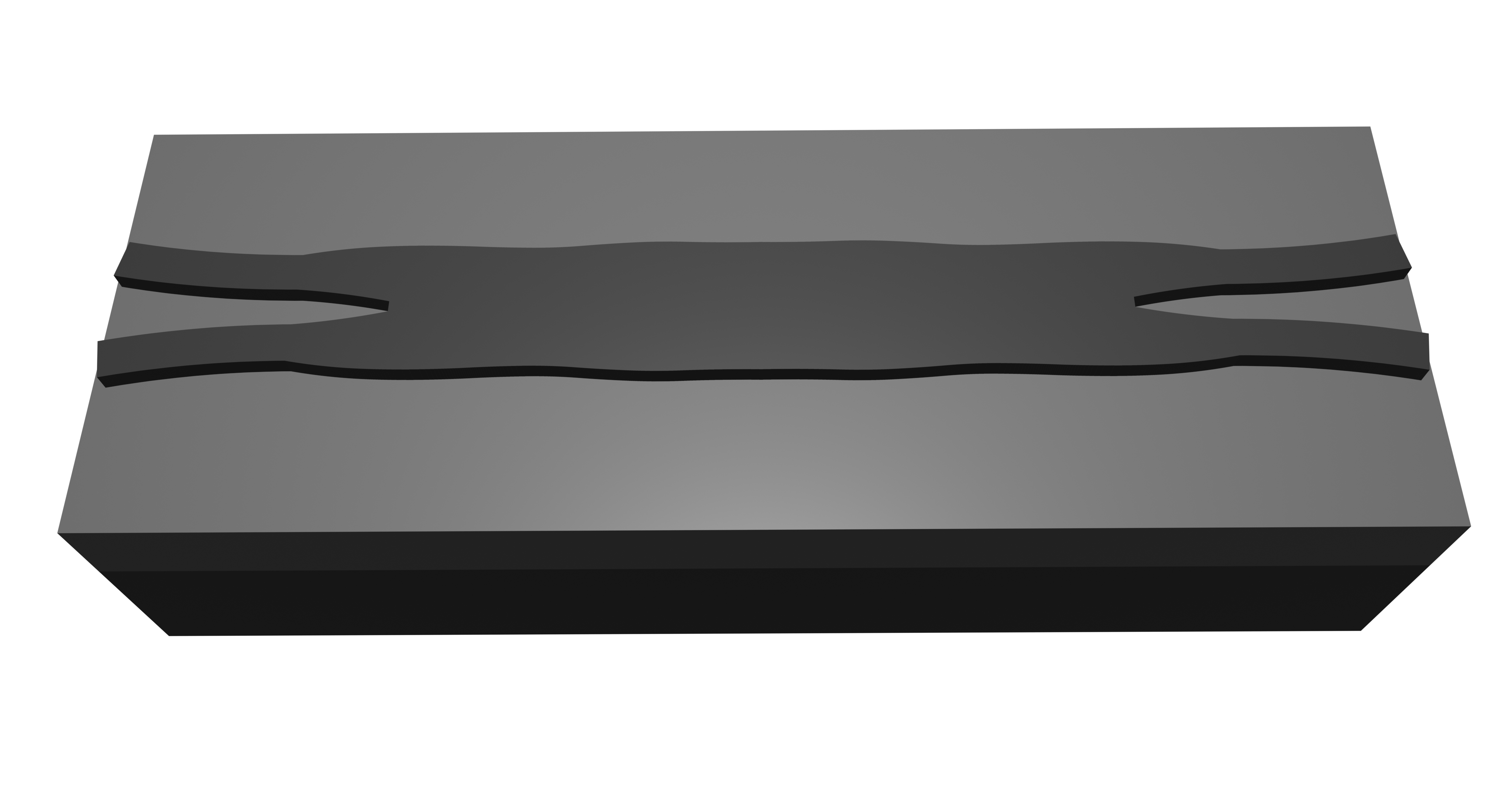
We experimentally demonstrate compact, low-loss, and broadband 2×2 Si optical couplers on a Si photonic platform designed using the covariance matrix adaptation evolution strategy (CMA-ES). The measured minimum insertion losses (ILs) in the C-band were 0.071 dB, 0.016 dB, 0.016 dB, and 45%–55% optical bandwidth were 140 nm, 136 nm, and 139 nm for device lengths of 7.56 μm, 9.64 μm, and 12.32 μm, respectively. The ILs are smaller than ever reported in 2 × 2 optical couplers shorter than 10 μm, and the optical bandwidths are much larger than a conventional directional coupler. The results validate the effectiveness of the proposed CMA-ES-based design method, extending the scope of application of our design method to the design of passive devices on Si photonics platform.
@article{MIYATAKE_2024_JJAP,doi={10.35848/1347-4065/ad983b},url={https://doi.org/10.35848/1347-4065/ad983b},year={2024},month=dec,publisher={IOP Publishing},volume={63},number={12},pages={12SP16},author={Miyatake, Yuto and Toprasertpong, Kasidit and Takagi, Shinichi and Takenaka, Mitsuru},title={Compact, low-loss, and broadband 2×2 Si optical coupler designed by covariance matrix adaptation evolution strategy},journal={Japanese Journal of Applied Physics},}
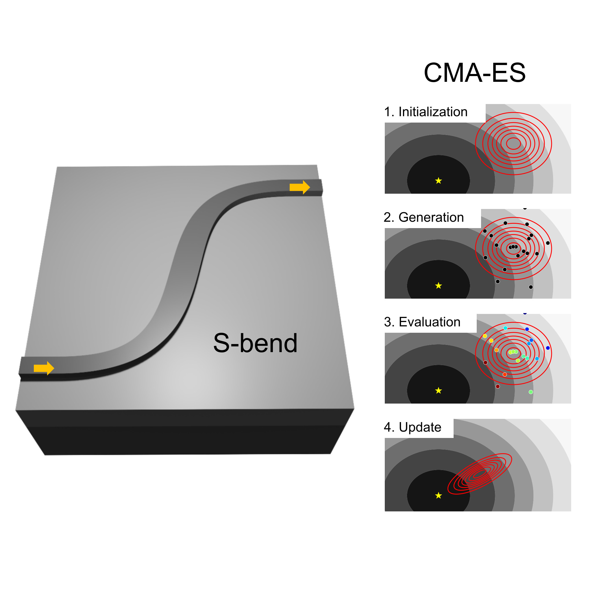
We employ the covariance matrix adaptation evolution strategy (CMA-ES) algorithm to design compact and low-loss S-bends on the standard silicon-on-insulator platform. In line with the CMA-ES-based approach, we present experimental results demonstrating insertion losses of 0.041 dB, 0.025 dB, and 0.011 dB for S-bends with sizes of 3.5 \textmum, 4.5 \textmum, and 5.5 \textmum, respectively, which are the lowest insertion losses within the footprint range smaller than approximately 30 \textmum2. These outcomes underscore the remarkable performance and adaptability of the CMA-ES to design Si photonics devices tailored for high-density photonic integrated circuits.
@article{MIYATAKE_2023_OE,author={Miyatake, Yuto and Toprasertpong, Kasidit and Takagi, Shinichi and Takenaka, Mitsuru},journal={Opt. Express},keywords={Coupling efficiency; Genetic algorithms; Inverse design; Neural networks; Optical modulators; Photonic crystals},number={26},pages={43850--43863},publisher={Optica Publishing Group},title={Design of compact and low-loss S-bends by CMA-ES},volume={31},month=dec,year={2023},url={https://opg.optica.org/oe/abstract.cfm?URI=oe-31-26-43850},doi={10.1364/OE.504866},}
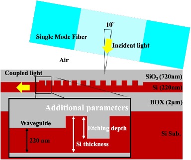
We examined the applicability of neural networks (NNs) and the covariance matrix adaptation evolution strategy (CMA-ES) for designing high-efficiency grating couplers on a Si-on-insulator (SOI) photonics platform operating at a wavelength of 1550 nm. We trained a NN to predict the wavelength dependences of coupling efficiency instead of using the finite-difference time-domain method, which enabled us to calculate analytically the gradient of coupling efficiency with respect to the design parameters. As a result, we found that a gradient-based method can be applied to find a more optimal design from an apodized grating coupler. In contrast, the CMA-ES, which is one of the most efficient evolutionary strategies, enabled us to explore a large design-parameter space efficiently without any constraint in an initial design of a grating coupler. As a result, we successfully obtained the optimal design from a uniform grating coupler. The optimized grating coupler exhibited a coupling efficiency of 74.7% when the thickness of the Si layer is 220 nm. The CMA-ES also enabled us to optimize the thickness of the Si gratings simultaneously. Through the optimization, we achieved a coupling efficiency of 92.1% when the Si thickness is 293 nm.
@article{MIYATAKE_2020_JJAP,doi={10.7567/1347-4065/ab641c},url={https://doi.org/10.7567/1347-4065/ab641c},year={2020},month=mar,publisher={IOP Publishing},volume={59},number={SG},pages={SGGE09},author={Miyatake, Yuto and Sekine, Naoki and Toprasertpong, Kasidit and Takagi, Shinichi and Takenaka, Mitsuru},title={Computational design of efficient grating couplers using artificial intelligence},journal={Japanese Journal of Applied Physics},}